|
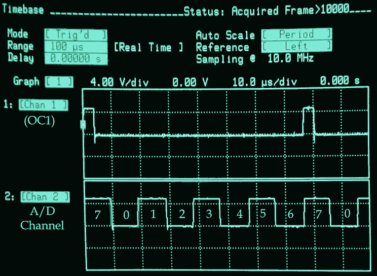
The 68HC16 microcontroller is very well suited to the O.I.F.T. task. However, at an early stage of design work for this project, it was discovered that the 68HC16 does have one near-fatal flaw. Its Analog to Digital Converter module does not have the capability to generate a CPU interrupt after a sequence of conversions is finished. This is a major disadvantage. Because of the high bandwidth required for the knock sensor, all of the analog signals must be sampled at a high rate. In fact, the A/D converter is set up for its highest possible rate (ADClock=2.1MHz) in the O.I.F.T. application. The problem lies in reliably retrieving the digital data. The ADC module continuously runs sequences of 8 conversions, one for each analog input. If we don't retrieve the digital data from the ADC module at a very specific time (when it's converting the last input) then the data from the first inputs may be overwritten by the next cycle's conversions. Using a polling routine is out of the question; there are too many things happening in the software for us to be able to meet all of the computational requirements of this project and meet the maximum latency requirements for the A/D converter using polling. And unfortunately, the ADC module lacks the capability to generate an interrupt. This seems to be a very tough problem. For a moment, all hope was lost. But then, from the depths of a twisted mind, came a more clever solution to this problem. The ADC module on the 68HC16Z1 has several different variables for controlling the sampling rate and conversion cycle rate. The ADClock is derived from the system clock with a configurable prescaler. With a system clock frequency of 25.17MHz, the lowest allowable value for this prescaler is 12, which gives an ADClock just under 2.1MHz. By setting the Final Sample Time to 2 ADClocks, the sampling frequency will be at its highest allowable value. At this rate the total conversion time for each input has been empirically observed to be 20 ADClock cycles (the manual however claims it is 18). So each A/D conversion will take 12 * 20 = 240 system clock cycles. And each cycle of 8 conversions will take 240 * 8 = 1920 system clock cycles. Here's where the clever bit comes in. An Output Compare ISR may be programmed to run at any frequency which can be generated by dividing the GPT frequency by an integer. The GPT itself is generated from the system clock with an 8-way prescaler. The GPT frequency may be set to a frequency equal to the system clock frequency divided by a power of two between 4 and 256, or an external clock may be selected. In order to achieve a nice balance between time resolution and counter overflow duration, a prescaler value of 2^6 (64) was selected. So the GPT clock runs at 25.17MHz / 64 = 393.216kHz, and has a period of 2.54us. Thus a 16-bit timer will overflow in 2.54us * 65536 = 1/6 second. So the lowest frequency measurable using the GPT timer is 6Hz. But back to the clever bit. For the O.I.F.T. application, the Output Compare 1 ISR is coded so that it fires every 30 GPT clock cycles. Since each GPT clock cycle is 64 CPU cycles, this interrupt (called the A/D Timer ISR) fires every 64 * 30 = 1920 clock cycles. That's the exact same frequency as the A/D conversion sequence. So if we can start the OC1 cycle and the A/D cycle at exactly the right times, then they should stay perfectly synchronized and the OC1 ISR may be used to reliably grab the A/D data at the right time with a minimum amount of overhead. So does all of this crazy stuff really work? You bet it does. Here's the initialization code, which completely sets up the GPT and ADC modules and waits for synchronization. JSR InitISR * Set the GPT Prescaler and interrupt mask LDAB #$08 ;0 0001 000 STAB TMSK1 ;IC/OC interrupts disabled except OC1 LDAB #$04 ;0 0 00 0 100 STAB TMSK2 ;TOI, PAOVI, PAII disabled. OC1 output normal ;GPT Prescaler = 64 * Set up the Input Capture and Output Compares ;do GPT module config (MCR) and interrupt config (ICR) registers LDD #$008E ;Give the GPT an IARB of $E so we can generate interrupts STD GPTMCR ;This priority must remain unique among modules LDD #$4640 ;elevate interrupt priority of OC1 IVBA:$4 , STD GPTICR ;set GPT IRQ level to 6 (high priority), ;& assign vector 64 (User vector 9) of the ;interrupt/exception vector table as the ;GPT's Interrupt Vector Base Address ;do pin control and OC1 control registers LDD #$F800 ;11111 000 00000000 STD PDDR ;OC1-5= output, IC1-3=input, output port = $00 LDD #$0808 ;00001 000 00001 000 STD OC1M ;set only OC1 pin high on OC1 match ;do timer control registers (i/o pin reaction) LDAB #$00 ;Output Compares: 00 00 00 00 STAB TCTL1 ;TOC5=off, TOC4=off, TOC3=off, TOC2=off LDAB #$00 ;Input Captures: 00 00 00 00 STAB TCTL2 ;TIC4=off, TIC3=off, TIC2=off, TIC1=off * Set up the A/D converter ;set module config register and Control Register 0 CLRD STD ADCMCR ;enable ADC operation LDD #$0085 ;00000000 1 00 00101 STD ADCTL0 ;10-bit, final sample time = 2 ADClock, prescale=/12 ;ADCTL1 will get set by the OC1 timer ISR when it fires the first time * Start the synchronized A/D and timer ;first, set the OC1 timer value LDD TCNT ;read the current timer value ADDD #$2 ;add 2 STD TOC1 ;set OC1 to happen real soon ;then, enable interrupts ANDP #$FF1F ;finally, wait for the OC1 routine to happen and start the A/D conversions InitL0: LDAA ADCSTAT ;read the ADC status register ANDA #$07 ;mask the conversion counter CMPA #$04 ;wait until AD input 4 is being converted BNE InitL0 ;just to make sure it's running ok And here's the code for the Output Compare 1 ISR and initialization routine: InitISR: CLRA STAA FD_ADTimerState,Z ;Set ADTimerState to zero RTS *------------------------------------------------------------------------------ * Output Compare 1 ISR (A/D Timer) OC1ISR: PSHM D ;save D on the stack LDAA FD_ADTimerState,Z BITA #$01 ;if ADTimerState is equal to 0 BEQ OC1ADStart ;then branch to OC1ADStart: OC1ISRTail: LDD TOC1 ;load value in Output Compare register ADDD #$1E ;Freq(GPT Timer) = 30 * Freq(A/D Conversion Cycle) STD TOC1 ;reset the Output Compare match value PULM D ;grab D back off the stack BCLR OC1D,#$08 ;force OC1 output to 0 BSET CFORC,#$08 BSET OC1D,#$08 ;reset OC1D to go high on OC1 again BCLR TFLG1,#$08 ;clear the OC1 interrupt flag bit RTI OC1ADStart: ;we need to start the A/D conversions LDD #$0070 ;000000000 1 1 1 0000 STD ADCTL1 ;start conversion. scan=1 mult=1 s8cm=1 LDD TOC1 ;load value in Output Compare register ADDD #$1A ;first cycle is just a bit short so that we'll ;arrive back at this ISR just as the conversion ;begins for the 7th input. Thus we have 2 A/D ;conversion times of headroom before result 0 gets ;overwritten STD TOC1 ;reset the Output Compare match value INC FD_ADTimerState,Z ;set ADTimerState to 1 PULM D ;grab D back off the stack BCLR TFLG1,#$08 ;clear the OC1 interrupt flag bit RTI The Main Loop for this piece of test software is deceptively simple, but provides a valuable service. This tiny piece of code continuously reads the ADCSTAT register, which contains a bit-field that holds the input channel number of the channel currently being converted. It then takes the lowest bit of this 3-bit field and rotates it to bit 7 before writing the resulting byte to Port E, which has been configured for output. An oscilloscope connected to bit 7 of Port E will then display the progress of the A/D converter. Here's the main loop code: Main0: LDAA ADCSTAT ;the Conversion Count is in the lowest 3 bits. RORA ;we shift bit 0 to bit 7 by rotating right twice. RORA STAA PORTE0 ;Now store this byte for output on Port E BRA Main0 ;Loop back forever The oscilloscope image below shows the resulting waveforms. Channel 1 is connected to the OC1 output signal (which goes high when the Output Compare 1 match is made and goes low when the OC1 ISR forces it low), and Channel 2 is connected to Port E bit 7. As the digagram below shows, the Output Compare 1 ISR always runs just after the A/D conversion begins for input channel 7. The OC1 ISR and A/D converter have been observed to stay in exact synchronization for periods of 12 hours or more.
The observant reader will note that it's impossible to verify consistent synchronization by watching a slow digital oscilloscope for 12 hours. This method only displays the lowest bit of the Conversion Counter, so it's not possible to visually see a difference between 0, 2, 4, and 6; or 1, 3, 5, and 7. However the test code also took care of this. In the actual test code which was used for this experiment, the OC1 ISR contained a small piece which read the Conversion Counter from the ADCSTAT register and would lock up the MCU by endlessly looping if the Conversion Counter was not equal to 7. The scope display would then "flatline" if the A/D converter lost synchronization with the OC1 ISR for any reason. And the experiment was successfully run continuously for more than 12 hours to prove that this solution works. |